Scanning Electron Microscope - Hitachi S-3500N
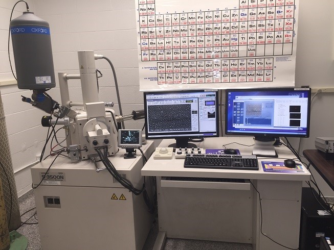
The Variable pressure 0.1-30 kV Hitachi S-3500N scanning electron microscope (SEM) is a fully digital instrument that provides high resolution (3.0nm) images of a sample by rastering a focused electron beam across the surface and detecting the secondary or backscattered electron signal. SEM can view specimens by secondary electron imaging, backscatter electron imaging, at high or low vacuum. The low vacuum mode, using the backscatter electron detector, allows viewing of unprocessed sample under Cryo or room temperature mode.
An energy dispersive X-ray analysis (EDX) system with 10 mm2 Si(Li) detector is attached to provide elemental identification, mapping and quantitative compositional information of a sample. All elements from atomic number 5 through 92 can be detected. The images produced by electrons collected from the sample reveal surface topography or mean atomic number differences according to the mode selected. This SEM is closely related to the electron probe and is designed primarily for producing electron images, but can also be used for element mapping, and even point analysis, if an X-ray spectrometer is added.
SEM is used in characterization of biological structures, particulates, defects, grain structure, aggregation effects, coating thickness on material structures, oxide films, glasses, ceramics, and polymers.
